Assembly of Intel’s first High-NA EUV machine starts shortly.
On Friday, Intel announced that it had received the first major components of ASML’s extreme ultraviolet (EUV) lithography tool. The two companies will begin assembling the machine shortly as Intel hopes to be the first company to use High-NA EUV equipment for mass production of chips in the coming years. The tool uses a 0.55 numerical aperture lens (High-NA), thus allowing chipmakers to print smaller features on processors than was previously possible. We previously covered ASML’s announcement last month that it had begun shipping the tool to Intel.
“Intel Oregon welcomes major components of ASML’s shipped High-NA EUV technology to help enable the continued and relentless pursuit of Moore’s Law,” a statement by Intel reads.
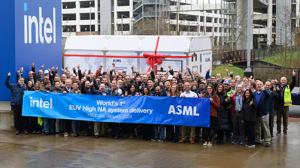
ASML’s Twinscan EXE lithography tool is a huge machine shipped in 250 crates spread across 13 cargo containers on 13 trucks. ASML sent the first container from Veldhoven, the Netherlands, on December 21 and now Intel received it at its site near Hillsboro, Oregon. In the coming months, the tool will be assembled at Intel’s D1X Mod3 research fab, where the company’s engineers will learn how to use the tool to produce chips using the company’s 18A fabrication technology.
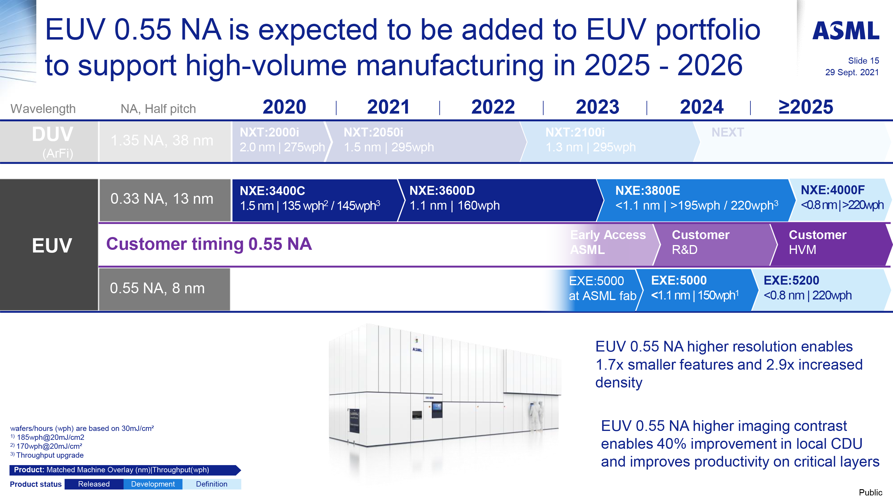
High-NA EUV litho machines are outfitted with a 0.55 NA (High-NA) lens that can achieve a resolution of 8nm, a major improvement over existing EUV tools — the existing 0.33 NA (Low-NA) lens offers a 13nm resolution. The resolution improvement will be crucial for post-2nm technologies requiring either Low-NA EUV double patterning or High-NA EUV single patterning. Each EUV High-NA scanner is expected to cost from $300 million to $400 million.

Intel will start installing the Twinscan EXE:5000 machine that can process 150 wafers per hour (at a dose of 30mJ/cm^2) with a <1.1nm matched-machine overlay performance. This machine will be used primarily to learn how to use High-NA EUV with Intel’s 18A (18 angstroms, 1.8nm) process technology, but the real high-volume manufacturing (HVM) will commence using a post-18A node on ASML’s Twinscan EXE:5200 machines. These machines will increase productivity to 220 wph and imaging performance to <0.8nm matched-machine overlay.
Intel wants to get back its fabrication technology leadership, and the company hopes to do so with 18A. With High-NA-enabled post-18A production nodes, Intel not only hopes to maintain power, performance, and area leadership but essentially establish its own standards when it comes to High-NA manufacturing. This could prove to be a strategic advantage over its rivals, much like TSMC’s pathfinding work with the first Low-NA machines helped it establish and maintain a lead over Intel.